Focused on the small things
Today, if a component of a jet or rocket engine calls for the alloy Inconel 718, technicians typically cast the shape of the part from this blend of mostly nickel and iron. They then machine it to create the precise size and shape required. Inconel 718 is exciting for engineers, because it is a “superalloy,” meaning it is notably strong and stable at high temperatures. Tim Smith, a materials research engineer at NASA’s Glenn Research Center in Ohio, wants to show how the highest grades of Inconel 718 might soon be 3-D printed, also called additively manufactured. Rocket engine parts manufacturers could then build on those specifications, designing and printing parts more quickly, cheaply and accurately. Smith wants to create specifications defining the optimal size and distribution of the strength-enhancing nanoparticles that a component made from additively manufactured Inconel 718 must have. The trouble is, he can’t see the nanoparticles well enough.
“It’s been really difficult to figure out what size these particles are, and how much of the volume of the metal is made up of those little particles, because of how small they are,” Smith says.
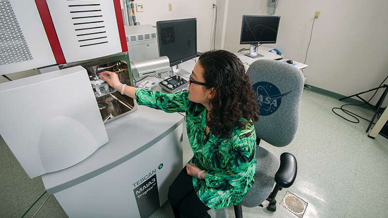
All that could soon change for Smith and other NASA materials researchers who face similar dilemmas. In March NASA Glenn took ownership of a new $500,000 microscope built by Tescan Orsay Holding of the Czech Republic.
The innovations inside the microscope, a model called MAIA3, deliver twice the resolution of any of the other seven microscopes at NASA Glenn, some of which are 20 years old. That should open the door to all sorts of possible new applications ranging from 3-D printing of Inconel 718 parts potentially for NASA’s Space Launch System rocket to surprising uses for aerogels, a class of lightweight materials typically made from silica and alumina. Scientists have yet to see the porous nanoscale structures of aerogels in clear detail.
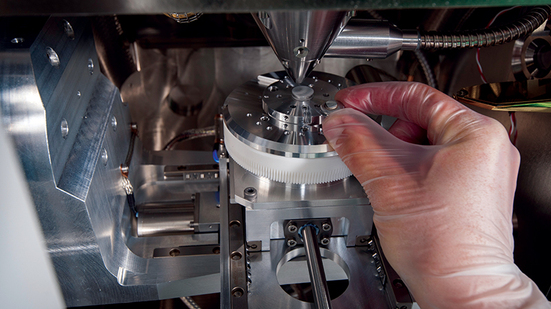
All scanning electron microscopes, including the Tescan MAIA3, work fundamentally the same way: They scan the viewed sample with an accelerated beam of electrons, focused by electromagnetic lenses, much like the optical lenses on a light microscope. The sample emits secondary electrons, which the microscope detects and turns into an image that the viewer sees on a computer screen. The new microscope’s resolution ranges down to 0.7 nanometers at 15 kiloelectron volts, a measure of the strength of the electron beam.
Here’s the challenge: Materials with low-conducting qualities will hold a charge from the electrons in the scanning beam. The electrons creating that charge in the material can then deflect other electrons from that incoming beam. This phenomenon deflects electron emissions and distorts the image. Designers of the MAIA3 solved that issue by empowering the user to choose a partial vacuum mode. Normally an electron microscope will create a vacuum in the viewing chamber so gas molecules don’t interfere with the incoming electrons’ path, making the electrons easier to focus. But for low-conducting materials, that vacuum condition encourages them to hold a charge. With the MAIA3, a user can elect to leave some gas in the chamber and these molecules carry some of the charge away from the material.
The new microscope’s software can also create high-resolution images at a lower electron beam strength, which is another way to improve viewing for low-conducting materials. This is done by decelerating the beam and decreasing the energy of the electrons so they don’t interact as much with the surface of the sample. This way the microscope can more tightly focus the beam. The new microscope’s designers promise a resolution of 1 nanometer at 1 kiloelectron volts for non-conductive materials, which is one of the main reasons NASA purchased it, says Laura Evans, NASA Glenn’s electron optics lab lead.
Fran Hurwitz, a senior materials research engineer at NASA, expects the new microscope to give her clear views for the first time of the critical structures in certain aerogels made of silica and alumina. Hurwitz is working on aerogels with a spongelike structure consisting of 94 percent or more air. If you could take a gram of this aerogel and spread its sponge structure flat, it would cover 400 square meters. The pores within the structure are just 10 to 50 nanometers wide and must be viewed at a magnification of 60,000 to 100,000 times. These aerogels tend to hold the charge from the microscope, masking the view of their structures.
Usually, to view a low-conducting material under an electron microscope, the sample is coated with gold or palladium, which becomes the electrical conductor. But for an aerogel, under 100,000 magnification, the viewer starts seeing the structure of the gold metal, which masks the structure of the aerogel, Hurwitz says.
When she views an aerogel under an older electron scanning microscope, she can’t slow the scan to get a high resolution image because doing so would cause a charge to build up in the material, which distorts the view so the structure looks solid, she says. So she directs the microscope in a rapid scan, which shows the pores, but she can only view the structure through screen shots.
“Right now, we’re playing a balancing game on a scope that’s maybe 17 years old,” Hurwitz says. “With the older microscopes, we’re using very low emission currents, and very low accelerating voltages and very short working distances, so we do all the things you’re not supposed to do to image a sample.”
Aerogels have physical and thermal properties based on their pore size and pore distribution, so the imaging helps the materials engineers to compare different aerogel formulations and their pore structures to the specific properties they are screening for. In some applications aerogels function as insulators by making it difficult for gas molecules to pass through their pores. Examples are seals or gaskets around cargo doors or engines, or heat insulation, or insulation for thermal electric devices, or protecting structures from fires. Aerogels are potentially valuable for space vehicle applications because they are extremely lightweight.
In theory, researchers could control the insulation properties of the material by manipulating the pore shapes and sizes. The engineers are also studying how the pore sizes change when they heat-treat the aerogels, a possible step in turning aerogels into high-temperature insulators. Specifically, they want to see if the pore structure might predict changes in thermal conductivity, density and shrinkage, Hurwitz says.
Another potential application would be for decelerating a spacecraft that is entering the atmosphere of Earth or other planet. The aerogel could be folded and packed into a small space, then inflated by an attached gas membrane to act as a reverse umbrella to slow descent while also acting as a heat shield.
“We’re trying to push the temperatures as high as we can,” Hurwitz says. The engineers formulated an aerogel that withstood exposure to 1,100 degrees Celsius temperatures for 96 hours, and 1,200 degrees for 24 hours without collapsing the pore structure.
For superalloy research, the NASA engineers will create 3-D printed parts, like those that might form part of a rocket engine, from a powder form of Inconel 718. Parts makers at NASA’s Marshall Space Flight Center in Huntsville, Alabama, will superheat the powder with a laser to form the parts, layer by layer, as is typical in additive manufacturing. Then the Glenn engineers will examine the parts under the new microscope — checking for voids, fissures or other microscopic defects, for example. They will also measure the metal’s nanoscale properties against more conventionally made alloys, because a 3-D printed metal can be quite different than its die-cast version. The new microscope can produce 3-D images, or anaglyphs, in real time, created from images taken from two slightly different angles and viewed by the microscope user through 3-D glasses, which can make it easier for the viewer to see deformities and cracks in the microscopic structures.
By checking the Inconel 718’s properties at each step, the engineers hope to develop specifications of optimal properties as a starting point for parts manufacturers to develop their own standards and steps for production. Among the critical properties are tensile strength and fatigue. “We’re doing work upfront so they don’t have to start from scratch,” says Peter Bonacuse, the analytical science group lead at NASA Glenn.
The NASA engineers will view the nanoscale particles dispersed in the Inconel 718. These serve a strengthening role similar to that of the bits of sand or gravel in concrete. The nanoparticles in this case provide strength and help prevent the part from deforming at high temperatures. Fatigue and creep are among the concerns. By noting the volume and size of those particles, and how those figures correspond to measurements of the strength of that version of the metal, the engineers can determine the optimal blend of the nanoscale particles.
Inconel 718 has two different shapes of nanoparticles. Some are spherical with a typical radius of 2 to 5 nanometers. These particles are either nickel-aluminum or nickel-titanium. Inconel 718 also has nickel-niobium particles that are plate-shaped with a radius of about 15 nanometers. With the sub-nanometer resolution of the new microscope, the scientists hope to distinguish between the two shapes, Smith says.
With the resolution of the older microscopes, scientists could “maybe get a sense” of the particles in the superalloy, but they couldn’t measure or quantify the particles reliably in terms of their size, he adds.
“Hopefully with the new scope we can actually give them a value. Something that’s important about that: If we have numbers that we trust, we can then work on producing models that predict their size and volume fractions so we can now calibrate these models because we have numbers that we can trust experimentally.”
The scientists are also additively manufacturing Inconel 718 tensile bars that they will test for yield strength and fatigue. The variable in their testing is the powder. They create it in different batches with slightly different chemistries, and when the parts are 3-D printed the different batches create different microstructures with different distributions of the nanoparticles. They hope to find the optimum powder chemistry that produces the strongest version of the superalloy, and identify that version by its nanoparticle characteristics.
The work is expected to go quickly now that the new telescope has arrived. Fundamental research is expected to wrap up in 2018 or 2019.
“It’s been really difficult to figure out what size these particles are, and how much of the volume of the metal is made up of those little particles, because of how small they are.”